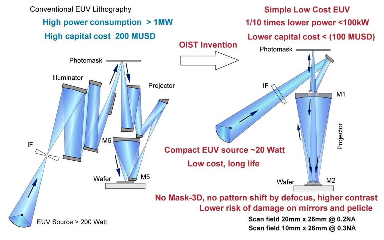
Japanese Simplified EUV Scanner for Cheaper Chip Production
Professor Tsumoru Shintake from the Okinawa Institute of Science and Technology (OIST) has introduced a revolutionary and simplified EUV lithography tool. This new device is less expensive than those produced by industry giant ASML, and if it reaches mass production, it could significantly impact the chipmaking equipment industry and the broader semiconductor sector.
Simplified Optical Projection Setup
The new system utilizes only two mirrors in its optical projection setup, a major shift from the traditional six-mirror configuration. Aligning these mirrors in a straight line ensures high optical performance without the usual distortions associated with EUV light. This optimized optical path allows over 10% of the initial EUV energy to reach the wafer, compared to about 1% in conventional systems, marking a substantial breakthrough.
Key Technological Advancements
Professor Shintake's team has addressed two major challenges in EUV lithography: preventing optical aberrations and ensuring efficient light transfer. The 'dual-line field' method developed by OIST illuminates the photomask without disrupting the optical path, minimizing distortions and enhancing image precision on silicon wafers.
Advantages of the Minimalist Design
This minimalist design not only enhances reliability and reduces maintenance complexities but also significantly lowers power consumption. The optimized optical path enables the system to operate with an EUV light source of just 20W, resulting in total power consumption of less than 100kW. In contrast, traditional EUV systems often require over 1MW of power. The reduced power consumption eliminates the need for a sophisticated and expensive cooling system.
Performance and Commercial Potential
The performance of this new system has been rigorously verified using optical simulation software, confirming its capability to produce advanced semiconductors. OIST has filed a patent for this technology, indicating its readiness for commercial deployment. The institute is committed to advancing the design further, aiming to bring it to practical application. This innovation is seen as a crucial step toward addressing global challenges related to the cost of chip production and the environmental impact of semiconductor fabs.
Economic Implications
The economic implications of this invention are promising. The global EUV lithography market is expected to grow from $8.9 billion in 2024 to $17.4 billion by 2030. The simplified design of EUV tools could lead to wider adoption of these systems in the coming years. However, the timeline for the commercialization of OIST's tool remains unclear.


